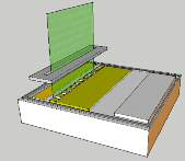
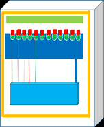
CSIC has developed a pixelated direct sensor to capture high-resolution images using electron microscopes. Each pixel of the sensor uses more than one electrode to measure the charge generated, and the output of the sensor comprises values of intensity and energy of the electrons that impact the sensor. This enriched representation is very useful for taking images or spectra of materials with high dynamic range, and to extract chemical information.
Industrial partners are sought to collaborate through a patent licence agreement.
New sensor for electron microscopy, built in standard CMOS technology, allows the incorporation of extra functionality with reduced costs Several applications in the field of electron microscopy (SEM or TEM) make use of the detection and accumulation of electrons in order to form images or energy spectra, which in turn are used for studying physical and chemical properties of materials. With the aim of acquiring images, electron microscopes are equipped with indirect electron sensors that are fabricated with pixelated semiconductors. Electrons are converted into photons by opto-coupling and then the detectors use either CCD or CMOS technologies for sensing photons. Indirect sensors typically have a low quantum efficiency and a poor modulation transfer function (MTF), degrading the quality of images and spectra. To improve them, it would be necessary to increase the capture times, not being the best strategy in samples, such as biological samples, susceptible to being damaged during the observation process. Thereafter, there is great interest in the design of direct pixelated sensor. At present, the state-of-the-art of direct sensors requires unconventional fabrication steps, or having a reduced number of pixels. In order to improve the MTF they must operate in counting mode (detecting and counting individual impacts of electrons).
Because of the geometry of the sensor, the pixel readout electronics is separated from the area of impact of the high energy electrons, thus avoiding that the circuitry of the sensor gets damagedThe sensor is direct, i.e., it can measure the high-energy electrons in an electron microscope without their prior conversion into low-energy photons what improves the quantum efficiency, and the modulation transfer function is closer to 1 within a wider range of spatial frequencies. Therefore, it can acquire images of greater quality using shorter exposure times what is very important for studying materials that are sensitive to radiation damage, especially biological materials.
The developed sensor allows to improve the quality of the images, both in counting mode and integration modes, in electronic microscopes, overcoming all the drawbacks indicated.
Main innovations and advantages
· The sensor is linear, with only one line of 2048 pixels. The image is formed by acquiring successive lines while scanning the imaging area in the transversal direction of the sensor.


